Automatic Inline Laser Soldering Equipment for Optical Device
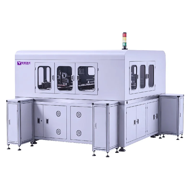
The automatic inline laser soldering equipment is a precision automated soldering system designed for optical device/optical module packaging production lines. It is equipped with a semiconductor laser soldering system, loading/unloading system, CCD vision positioning system, bonding module, AOI module, dispensing module, fixture exchange and return module, and unloading module, etc. It integrates automatic loading, positioning, laser soldering, vision inspection, and unloading functions.
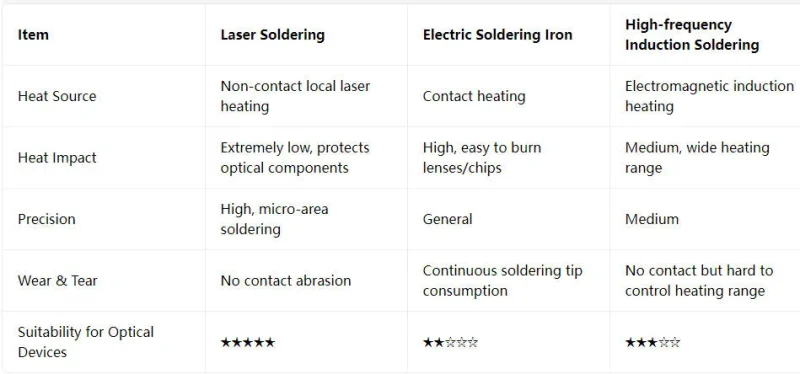
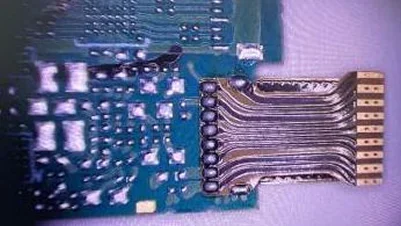
It adopts a non-contact laser heat source with an extremely small heat-affected zone, solving the industry pain point that heat-sensitive chips, optical coatings, and lenses in optical devices are susceptible to thermal damage. It meets the mass production requirements of high-speed optical modules for small size, high precision, and high reliability.
Low heat input: Localized fixed-point heating with a small heat-affected zone, protecting lenses, PD/LD chips, and optical coatings, reducing device failure risk, and outperforming traditional soldering irons and induction soldering.
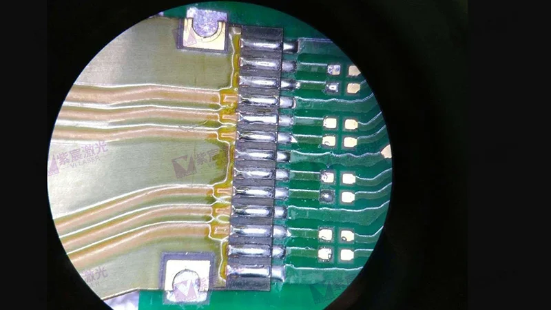
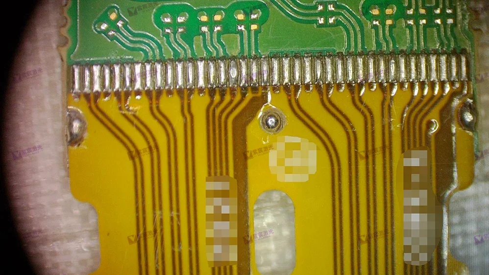
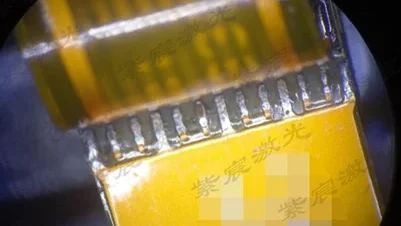
High-precision micro soldering: Micron-level positioning, suitable for soldering in confined spaces and with ultra-fine pin pitches, with good solder joint consistency.
Non-contact soldering: No probe/soldering iron tip contacts the workpiece, eliminating wear and compression damage to optical surfaces, and reducing tooling loss.
Automated integration: Can interface with upstream and downstream processes, with automatic loading/unloading, reduced manual intervention, and stable yield, suitable for mass production of optical modules.
Strong process flexibility: Rapid program switching, compatible with multiple optical device products; solder joint trajectories can be flexibly edited, enabling both single-point and continuous soldering.
Traceability: Soldering parameters and yield data for each product are automatically saved, meeting the reliability control requirements of the communications industry.