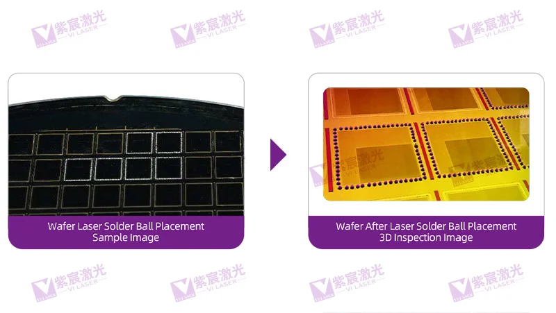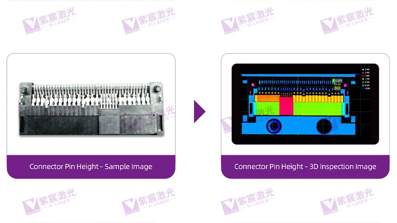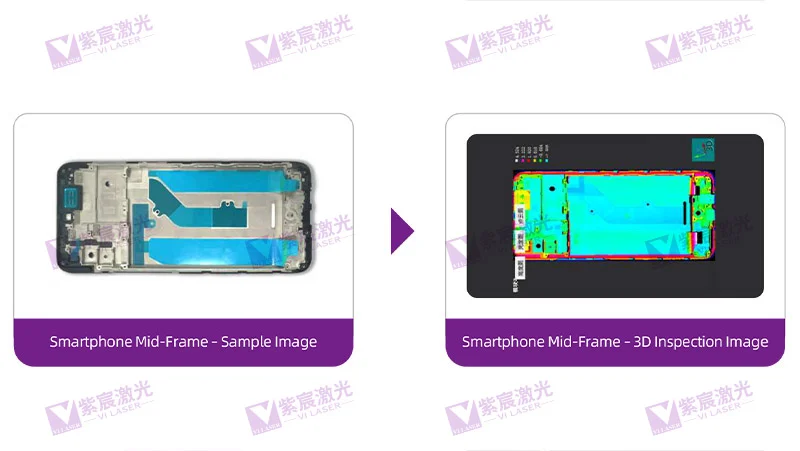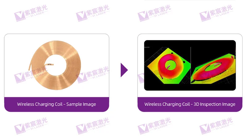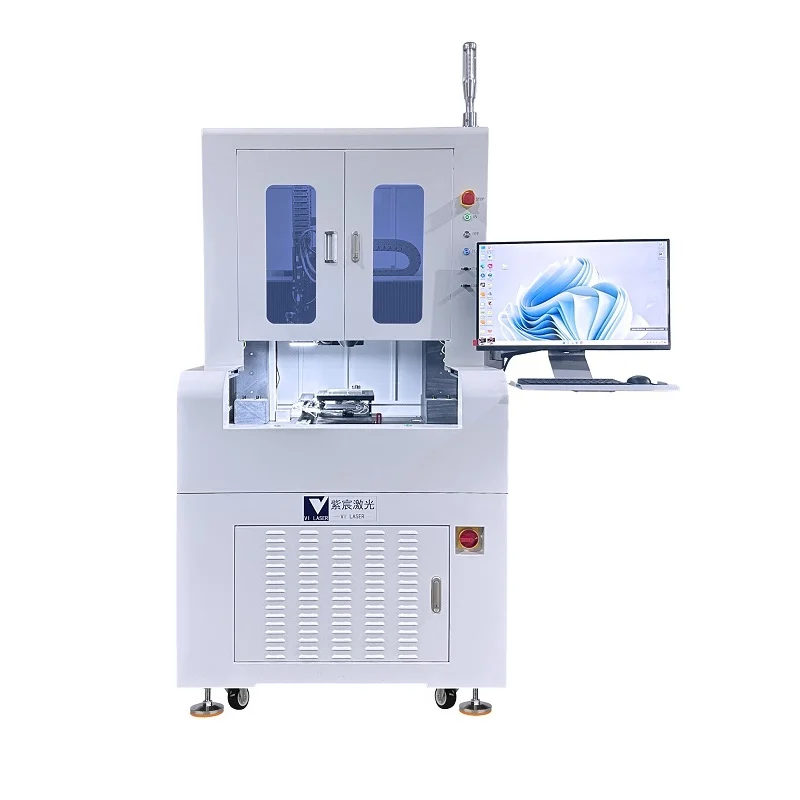

The 3D Inspection System is mainly applied in PCB, FPC, semiconductor packaging and precision electronics manufacturing sectors for dimension measurement, topography analysis and defect inspection. Supporting multiple 3D inspection technologies including 3D camera, line laser and line spectroscopy, the system enables flexible configuration of inspection solutions according to product characteristics. It performs solder joint topography inspection, dimension measurement and structural defect judgment to realize non-contact 3D inspection of precision workpieces and quantify product quality data.
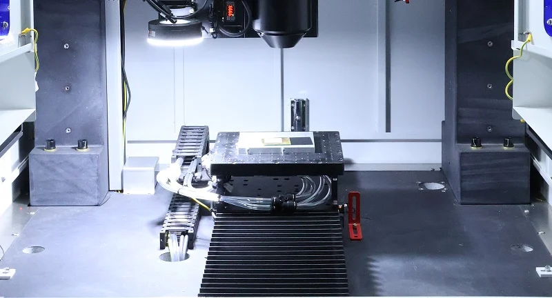
Non-contact 3D inspection prevents scratches on precision electronic components and solder joints. It captures the true 3D contour of workpieces. Unlike conventional 2D vision, it can detect 3D defects that are hard to identify in 2D images, such as height difference, warpage, cold solder joints, dents and bulges. Inspection data is digitally archived to facilitate process review and full-lifecycle product traceability. The system can be integrated into automatic production lines for on-line inspection.
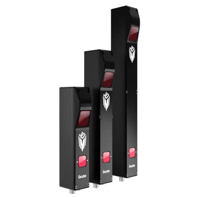
Supports 3D camera, line laser, line spectroscopy and other inspection modes. Selection can be flexibly made based on workpiece materials and inspection accuracy requirements.
Capable of solder joint topography observation, product height measurement, critical dimension inspection and identification of various structural defects.
Displays inspection results in real time, automatically conducts result judgment and yield statistics. Inspection files can be saved and archived for quality traceability.
Built-in library of over 150 2D/3D vision tools. Inspection templates can be quickly created to adapt to different products and inspection tasks, delivering high product changeover efficiency.