
Semiconductor
Semiconductor
Semiconductor

With the rapid development of artificial intelligence, high-performance computing and smart terminals, the semiconductor industry continues to evolve towards high integration, high performance and advanced packaging.

In chip packaging and electronic manufacturing, micro-connectivity, precision machining, and quality inspection are crucial for ensuring product performance. With continuously shrinking package sizes, increasing I/O counts, and rapid advancements in advanced packaging technologies, traditional processing methods face greater challenges in handling microstructures, controlling thermal impacts, and ensuring manufacturing consistency.

In the manufacturing processes of advanced packaging, power devices, and semiconductor-related components, high-precision and high-stability intelligent equipment is required to meet the needs of complex structure processing and large-scale production.

VI LASER solutions

To meet the needs of semiconductor packaging and precision electronics manufacturing, Zichen Laser provides laser intelligent equipment solutions covering precision connection, micro-machining and inspection processes.

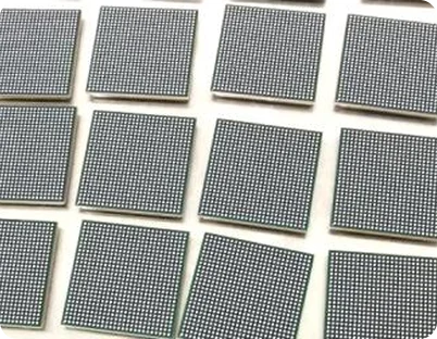
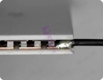
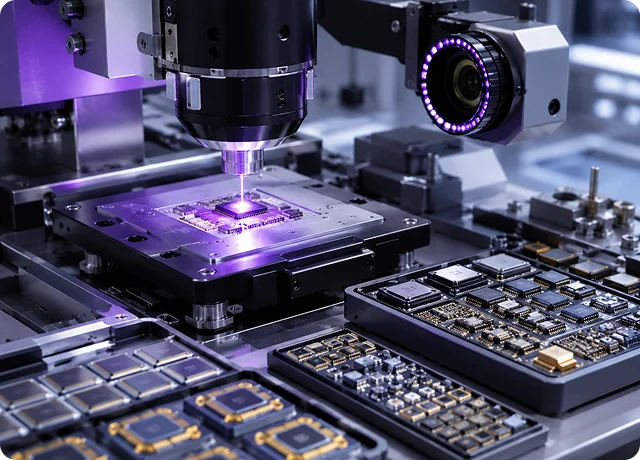
In the micro-connect manufacturing process, the company's laser solder ball, solder wire and solder paste welding equipment can be applied to chip packaging, electronic component connection and high-density welding scenarios to achieve stable processing and consistency control of tiny solder joints.

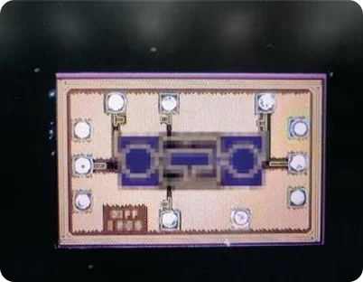
In precision machining, laser cutting, drilling, and etching technologies can be used to process ceramic substrates, packaging structures, and precision parts, meeting the needs of complex structures and micro-machining.

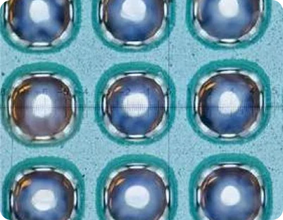
Meanwhile, 3D vision inspection technology is used to inspect and analyze the solder joint morphology, dimensional accuracy, and processing results, providing quality assurance for the semiconductor manufacturing process.

Rectangle 346242845
Main application directions

Designed for chip packaging and high-density interconnection, enabling precise processing of micro-scale solder joints to improve connection reliability and production consistency.

Supports high-precision cutting, drilling, and structural processing for ceramic substrates, packaging carriers, and other precision components.

3D vision inspection enables analysis of critical dimensions, surface morphology, and welding quality, improving quality control throughout the semiconductor manufacturing process.

Our Partners
Sample Display
Image 1812 (1)
xxxxxx
Image 1815 (1)
xxxxxxx
Image 1814 (1)
xxxxxx
Image 1813 (1)
xxxxxx

Free Sample

Get a Quote